

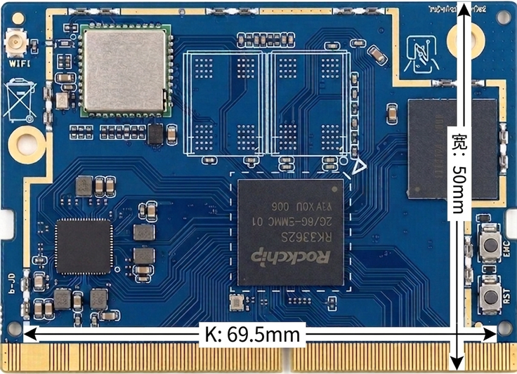
The RK3326S-V02 Standard Core Board utilizes the RK3326-S as its main CPU, The functional block diagram of the chip is shown below:


Top View

Bottom View
| Width | 50mm |
| Length | 69.5mm |
| Tolerance | ±0.5mm |
The basic parameters are listed in the table below:
| Name | Description |
|---|---|
| SoC | Rockchip RK3326-S |
| CPU | Quad-core 64-bit Cortex-A35 processor, up to 1.5 GHz |
| GPU | Mali-G31 2EE GPU Support OpenGL ES3.2, Vulkan 1.0, OpenCL 2.0 Embedded high-performance 2D graphics acceleration hardware. |
| Multimedia | Multi-format 1080p @ 60 fps video decoding (H.265, H.264, VC-1, MPEG-1/2/4, VP8). 1080p video encoding , support H.264, VP8. |
| Memory | LPDDR4/LPDDR4x,default 1GB |
| Storage | EMMC, default 32GB |
| Display Interface | Supports RGB, LVDS, and MIPI-DSI interfaces with a maximum resolution of 1920×1080. |
| Audio Interface | 1 × HPR/L, Stereo Headphone Output 1 × SPK 1 × MIC Microphone Inputs |
| USB | 1 × USB2.0 OTG |
| Expansion Connector | 4 × UART 2 × SPI 3 × I2C 2 × I2S PCM(2ch) 1 × I2S TDM(8ch) 1 × SDIO 2 × PWM 1 × ADC |

| NO. | Description |
|---|---|
| 1 | IPEX Gen 1 Connector |
| 2 | RK3326S BOOT Button |
| 3 | RK3326S Reset Button |

Core Board Interface – Odd Pin Definitions (Refer to the SoC Datasheet for detailed pin multiplexing functions.)
| Pin No. | Connector Label | Description |
|---|---|---|
| 1 | GND | GND |
| 3 | GND | GND |
| 5 | GND | GND |
| 7 | SYS_5V0 | SYS_5V0 |
| 9 | SYS_5V0 | SYS_5V0 |
| 11 | SYS_5V0 | SYS_5V0 |
| 13 | SYS_5V0 | SYS_5V0 |
| 15 | SYS_5V0 | SYS_5V0 |
| 17 | SYS_5V0 | SYS_5V0 |
| 19 | SYS_5V0 | SYS_5V0 |
| 21 | SYS_5V0 | SYS_5V0 |
| 23 | - | - |
| 25 | - | - |
| 27 | GND | GND |
| 29 | GND | GND |
| 31 | GND | GND |
| 33 | VCC3V3_SYS | VCC3V3_SYS |
| 35 | VCC3V3_SYS | VCC3V3_SYS |
| 37 | VCC3V3_SYS | VCC3V3_SYS |
| 39 | - | - |
| 41 | - | - |
| 43 | - | - |
| 45 | VCC_3V0 | VCC_3V0 |
| 47 | VCC_3V0 | VCC_3V0 |
| 49 | - | - |
| 51 | - | - |
| 53 | - | - |
| 55 | GND | GND |
| 57 | - | - |
| 59 | - | - |
| 61 | - | - |
| 63 | - | - |
| 65 | - | - |
| 67 | - | - |
| 69 | GND | GND |
| 71 | CIF_CLKI | GPIO2_B2_d |
| 73 | GND | GND |
| 75 | CAM_CLKO | GPIO2_B3_d |
| 77 | GND | GND |
| 79 | CIF_D9 | GPIO2_A7_d |
| 81 | CIF_D8 | GPIO2_A6_d |
| 83 | CIF_VSYNC | GPIO2_B0_d |
| 85 | CIF_HREF | GPIO2_B1_d |
| 87 | CIF_D2 | GPIO2_A0_d |
| 89 | CIF_D5 | GPIO2_A3_d |
| 91 | CIF_D7 | GPIO2_A5_d |
| 93 | CIF_D4 | GPIO2_A2_d |
| 95 | CIF_D6 | GPIO2_A4_d |
| 97 | CIF_D3 | GPIO2_A1_d |
| 99 | GND | GND |
| 101 | USB_OTG_DM | USB_OTG_DM |
| 103 | USB_OTG_DP | USB_OTG_DP |
| 105 | GND | GND |
| 107 | USB_OTG_ID | USB_ID |
| 109 | USB_DET | USB_VBUS |
| 111 | GND | GND |
| 113 | I2S1_SCLK | GPIO2_C2_d |
| 115 | I2S1_MCLK | GPIO2_C3_d |
| 117 | I2S1_LRCK_TXRX | GPIO2_C1_d |
| 119 | I2S1_SDO | GPIO2_C4_d |
| 121 | GND | GND |
| 123 | SDMMC0_D3/JTAG_TMS | SDMMC0 Data 3 |
| 125 | SDMMC0_D2/JTAG_TCK | SDMMC0 Data 2 |
| 127 | SDMMC0_CMD | SDMMC0 Command Signal |
| 129 | SDMMC0_D1/UART2_RX | SDMMC0 Data1 |
| 131 | SDMMC0_D0/UART2_TX | SDMMC0 Data 0 |
| 133 | SDMMC0_CLK | SDMMC0 Clock Signal |
| 135 | SDMMC0_DET | GPIO0_A3 |
| 137 | GND | GPIO0_A3 |
| 139 | I2C1_SCL | I2C1 Clock Signal |
| 141 | I2C1_SDA | I2C1 Data Signal |
| 143 | GND | GND |
| 145 | GND | GND |
| 147 | GND | GND |
| 149 | GND | GND |
| 151 | GND | GND |
| 153 | GND | GND |
| 155 | GND | GND |
| 157 | GND | GND |
| 159 | GND | GND |
| 161 | GND | GND |
| 163 | GND | GND |
| 165 | LCDC_BL_PWM | GPIO0_C0_d |
| 167 | - | - |
| 169 | - | - |
| 171 | - | - |
| 173 | - | - |
| 175 | - | - |
| 177 | ADC0_HW_ID | ADC_IN0 |
| 179 | GND | ADC_IN0 |
| 181 | PHONE_DET | GPIO1_B5 |
| 183 | VCC18_LCD_EN | GPIO1_B7 |
| 185 | SPK_CTL_H | GPIO1_B6 |
| 187 | FLASH_CLE | GPIO1_B4_d |
| 189 | GND | GND |
| 191 | BT_PCM_CLK | GPIO3_A2_d |
| 193 | LCDC_D12 | GPIO3_C0_d |
| 195 | LCDC_D13 | GPIO3_C1_d |
| 197 | LCDC_D15 | GPIO3_C3_d |
| 199 | LCDC_D14 | GPIO3_C2_d |
| 201 | LCDC_D17 | GPIO3_C5_d |
| 203 | LCDC_D6 | GPIO3_B2_d |
| 205 | LCDC_D16 | GPIO3_C4_d |
| 207 | GND | GND |
| 209 | LVDS_MIPI_TXD0P | LVDS_MIPI_TXD0P |
| 211 | LVDS_MIPI_TXD0N | LVDS_MIPI_TXD0N |
| 213 | GND | GND |
| 215 | LVDS_MIPI_TXD1P | LVDS_MIPI_TXD1P |
| 217 | LVDS_MIPI_TXD1N | LVDS_MIPI_TXD1N |
| 219 | GND | GND |
| 221 | LVDS_MIPI_TXCLKP | LVDS_MIPI_TXCLKP |
| 223 | LVDS_MIPI_TXCLKN | LVDS_MIPI_TXCLKN |
| 225 | GND | GND |
| 227 | LVDS_MIPI_TXD2P | LVDS_MIPI_TXD2P |
| 229 | LVDS_MIPI_TXD2N | LVDS_MIPI_TXD2N |
| 231 | GND | GND |
| 233 | GND | GND |
| 235 | GND | GND |
| 237 | GND | GND |
| 239 | GND | GND |
| 241 | GND | GND |
| 243 | GND | GND |
| 245 | GND | GND |
| 247 | GND | GND |
| 249 | GND | GND |
| 251 | GND | GND |
| 253 | GND | GND |
| 255 | GND | GND |
| 257 | GND | GND |
| 259 | GND | GND |
Core Board Interface – Even Pin Definitions (Refer to the SoC Datasheet for detailed pin multiplexing functions.)
| Pin No. | Connector Label | Description |
|---|---|---|
| 2 | GND | GND |
| 4 | GND | GND |
| 6 | GND | GND |
| 8 | GND | GND |
| 10 | SPKP_OUT | SPK+ Speaker Positive Output |
| 12 | SPKN_OUT | SPK- Speaker Negative Output |
| 14 | GND | GND |
| 16 | GND | GND |
| 18 | MIC2_IN | MIC2- MIC2 Negative Input |
| 20 | MIC1_IN | MIC1+ MIC1 Positive Input |
| 22 | GND | GND |
| 24 | HPR | Headphone Right Channel Output |
| 26 | HPL | Headphone Left Channel Output |
| 28 | HP_SNS | HP_SNS |
| 30 | GND | GND |
| 32 | - | - |
| 34 | - | - |
| 36 | - | - |
| 38 | GND | GND |
| 40 | GND | GND |
| 42 | GND | GND |
| 44 | GND | GND |
| 46 | GND | GND |
| 48 | GND | GND |
| 50 | GND | GND |
| 52 | GND | GND |
| 54 | VCC1V8_DVP | VCC1V8_DVP |
| 56 | VCC2V8_DVP | VCC2V8_DVP |
| 58 | VDD1V5_DVP | VDD1V5_DVP |
| 60 | RESET | RESET |
| 62 | ADC1_HP_HOOK | ADC1_HP_HOOK |
| 64 | ADC2_KEY_IN | ADC2_KEY_IN |
| 66 | GND | GND |
| 68 | - | - |
| 70 | GND | GND |
| 72 | GPIO2_B4 | GPIO2_B4_d |
| 74 | I2C2_SDA_CAM | I2C2 Data Signal |
| 76 | CAM_PDN0 | GPIO2_B6_d |
| 78 | CAM_PDN1 | GPIO2_B5_d |
| 80 | I2C2_SCL_CAM | I2C2 Clock Signal |
| 82 | GND | GND |
| 84 | - | - |
| 86 | - | - |
| 88 | - | - |
| 90 | - | - |
| 92 | GND | GND |
| 94 | MIPI_CSI_D2P | MIPI_CSI_D2P |
| 96 | MIPI_CSI_D2P | MIPI_CSI_D2P |
| 98 | GND | GND |
| 100 | - | - |
| 102 | - | - |
| 104 | GND | GND |
| 106 | MIPI_CSI_D1N | MIPI_CSI_D1N |
| 108 | MIPI_CSI_D1P | MIPI_CSI_D1P |
| 110 | GND | GND |
| 112 | MIPI_CSI_D3N | MIPI_CSI_D3N |
| 114 | MIPI_CSI_D3P | MIPI_CSI_D3P |
| 116 | GND | GND |
| 118 | MIPI_CSI_D0N | MIPI_CSI_D0N |
| 120 | MIPI_CSI_D0P | MIPI_CSI_D0P |
| 122 | GND | GND |
| 124 | MIPI_CSI_CLKN | MIPI_CSI_CLKN |
| 126 | MIPI_CSI_CLKP | MIPI_CSI_CLKP |
| 128 | GND | GND |
| 130 | - | - |
| 132 | - | - |
| 134 | - | - |
| 136 | GPIO0_A0 | GPIO0_A0 |
| 138 | GND | GND |
| 140 | I2C0_SCL_PMIC | I2C0 Clock Signal |
| 142 | I2C0_SDA_PMIC | I2C0 Data Signal |
| 144 | GND | GND |
| 146 | GND | GND |
| 148 | GND | GND |
| 150 | GND | GND |
| 152 | GND | GND |
| 154 | GND | GND |
| 156 | GND | GND |
| 158 | GND | GND |
| 160 | GND | GND |
| 162 | TP_RST | GPIO0_B4_u |
| 164 | GPIO0_B5_u | GPIO0_B5_u |
| 166 | TP_INT | GPIO0_B3_d |
| 168 | SENSOR_INT | GPIO0_B7_d |
| 170 | GND | GND |
| 172 | LCDC_CLK | LCDC_CLK |
| 174 | GND | GND |
| 176 | - | - |
| 178 | - | - |
| 180 | BT_REG_ON | GPIO0_C1_d |
| 182 | GPIO1_B0 | GPIO1_B0 |
| 184 | GND | GND |
| 186 | COMP_INT | GPIO3_B4_d |
| 188 | RK618_PWREN | GPIO3_B0_d |
| 190 | BT_PCM_IN | GPIO3_A7_d |
| 192 | BT_PCM_OUT | GPIO3_A5_d |
| 194 | BT_PCM_SYNC | GPIO3_A3_d |
| 196 | DC_DET | GPIO3_A1_d |
| 198 | LCD_RST | GPIO3_B7_d |
| 200 | RK912_IRQ | GPIO3_B6_d |
| 202 | RK618_RST | GPIO3_B1_d |
| 204 | LCDC_D23 | GPIO3_D3_d |
| 206 | LCDC_D22 | GPIO3_D2_d |
| 208 | LCDC_D7 | GPIO3_B3_d |
| 210 | LCDC_D21 | GPIO3_D1_d |
| 212 | LCDC_D9 | GPIO3_B5_d |
| 214 | LCDC_D20 | GPIO3_D0_d |
| 216 | LCDC_D0 | GPIO3_A4_d |
| 218 | LCDC_D19 | GPIO3_C7_d |
| 220 | LCDC_D2 | GPIO3_A6_d |
| 222 | LCDC_D18 | GPIO3_C6_d |
| 224 | GND | GND |
| 226 | - | - |
| 228 | - | - |
| 230 | - | - |
| 232 | - | - |
| 234 | - | - |
| 236 | GND | GND |
| 238 | GND | GND |
| 240 | GND | GND |
| 242 | GND | GND |
| 244 | GND | GND |
| 246 | GND | GND |
| 248 | GND | GND |
| 250 | GND | GND |
| 252 | GND | GND |
| 254 | GND | GND |
| 256 | GND | GND |
| 258 | GND | GND |
| 260 | GND | GND |
 Home
 Product
 Inquiry
 Share